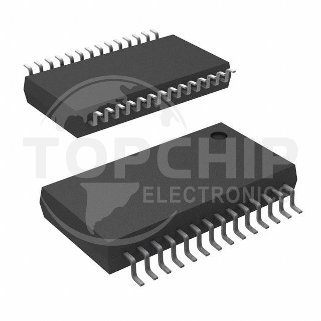
The ADS1256IDBR is a 24-bit Σ-Δ analog-to-digital converter from Texas Instruments. SMIC Juneng, which sells a full range of Texas Instruments' IC electronic components as an agent, will provide you with detailed explanations of ADS1256IDBR parameters, functional features, application fields, etc.
Detailed explanation of ADS1256IDBR Chinese parameters
Brand: Texas Instruments
Product Family: Data Acquisition - Analog-to-Digital Converters (ADCs)
Packaging: Tape and Reel (TR), Cut Tape (CT)
Part status: active
Digits: 24
Sample rate (per second): 30k
Number of inputs: 4, 8
Input type: Differential, single-ended
Data interface: SPI
Configuration:MUX-PGA-ADC
Ratio-S/H:ADC:-
Number of A/D converters: 1
Architecture: Trigonometric Calculus
Reference type: external
Voltage - Power supply, analog: 5V
Voltage - power supply, digital: 1.8V ~ 3.6V
Features: PGA
Working temperature: -40°C ~ 85°C
Product package: 28-SSOP (0.209, 5.30mm wide)
Supplier Device Package: 28-SSOP
ADS1256IDBR features
1. 24-bit resolution: Provides high-resolution analog-to-digital conversion, suitable for applications that require higher accuracy.
2. 8 single-ended/4 differential input channels: can meet a variety of signal acquisition needs.
3. Low noise: Built-in low-noise PGA (programmable gain amplifier) and Σ-Δ ADC, suitable for applications that require high signal quality.
4. Low power consumption: suitable for low-power applications that require long-term operation.
5. Internal/external reference voltage: Internal or external reference voltage source can be selected.
6. SPI interface: Use SPI interface to communicate with microcontrollers or other digital devices.
ADS1256IDBR application fields
1. Sensor interface: used to connect various analog sensors, such as temperature sensors, pressure sensors, etc.
2. Industrial automation: used for data collection and measurement in industrial control systems.
3. Medical equipment: Suitable for applications in medical equipment that require high signal accuracy and quality.
4. Instruments: used for precision measurement and data collection in various instruments.
ADS1256IDBR pin diagram and detailed explanation of pin functions
1. ADS1256IDBR pin diagram
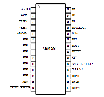
2. Detailed explanation of ADS1256IDBR pin functions:
1. AIN0-AIN7: Analog input channels, which can be connected to the signal source under test.
2. DVDD: digital power pin.
3. DGND: digital ground pin.
4. AVDD: Analog power pin.
5. AGND: Analog ground pin.
6. RESET: Reset pin, used to reset the chip.
7. PDWN: Power-down pin, used to control the power-down mode of the chip.
8. SCLK: Serial clock input pin.
9. SDATA: Serial data input pin.
10. SDO: Serial data output pin.
ADS1256IDBR working principle
ADS1256IDBR uses Σ-Δ modulation technology. Its working principle is to amplify the analog input signal through a PGA (programmable gain amplifier) and then send it to the Σ-Δ ADC for digital conversion. The converted digital signal can be output to a microcontroller or other digital device for processing through the SPI interface.
Instructions for use of ADS1256IDBR
1. Power supply: Connect the analog and digital power pins correctly to ensure that the chip works normally.
2. Analog input: Connect the signal under test to the analog input pin, and ensure that the signal range is within the specified working range of the chip.
3. Interface: Communicates with a microcontroller or other digital device through the SPI interface.
4. External components: Connect external components correctly according to the data sheet requirements, such as filter capacitors and reference voltage sources.